Chiplets and advanced packaging (2.5D/3D)
Building one processor from several smaller dies in a package; beats reticle and yield limits and mixes process nodes.
- 2011
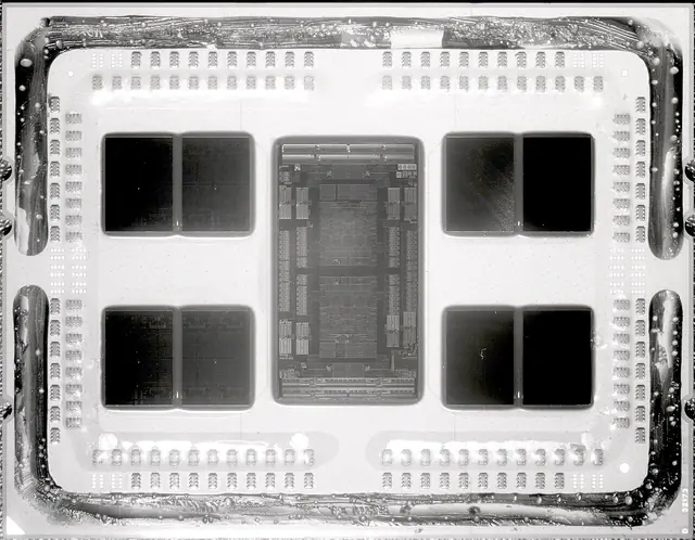
First version
Xilinx (2.5D interposer FPGA); popularised by AMD (Zen 2 chiplets)
Image: Fritzchens Fritz · CC0 · Wikimedia Commons - 2019
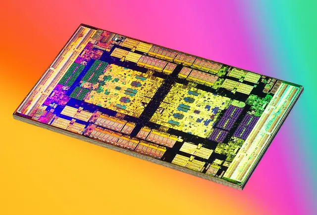
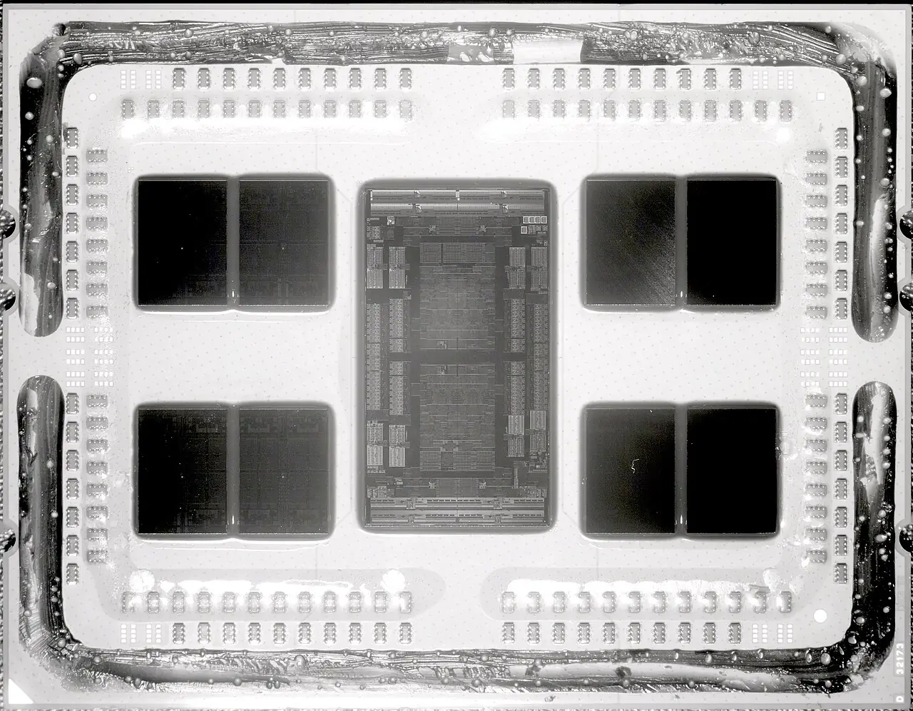
AMD EPYC Rome
Eight 7nm CPU chiplets around a 14nm I/O die: 64 cores per socket.
Image: Fritzchens Fritz · CC0 · Wikimedia Commons - 2022
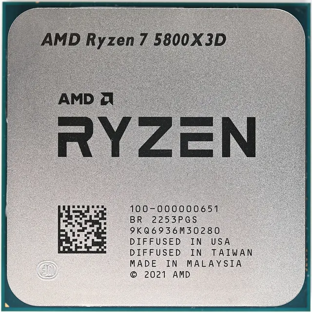
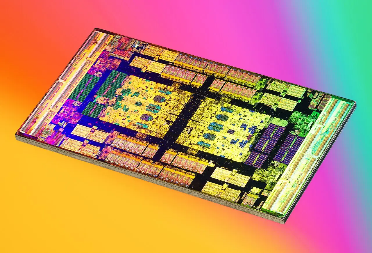
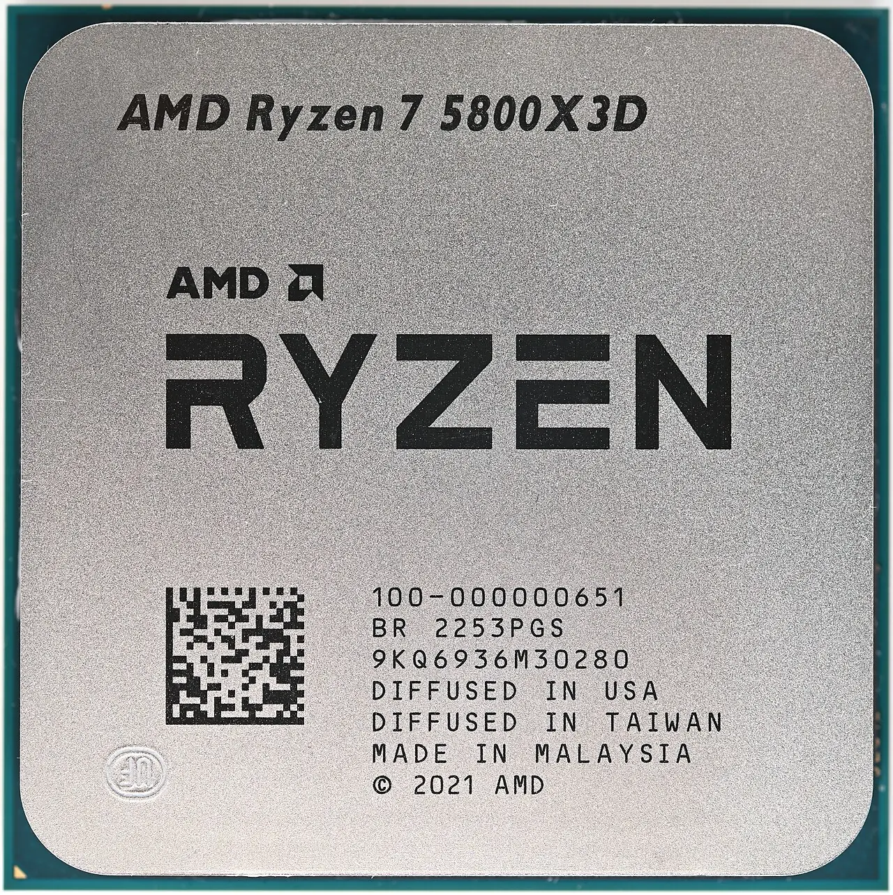
AMD 3D V-Cache
A 64MB cache die is bonded copper-to-copper, with no solder bumps, directly onto the CPU chiplet: hybrid-bonded 3D stacking reaches mass-market processors.
Image: Phiarc · CC BY-SA 4.0 · Wikimedia Commons - 2023
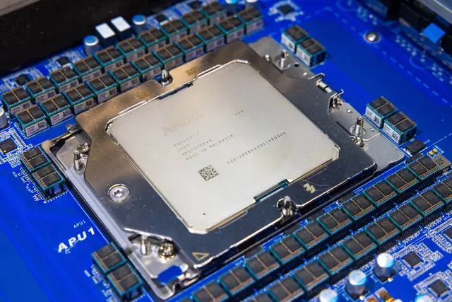
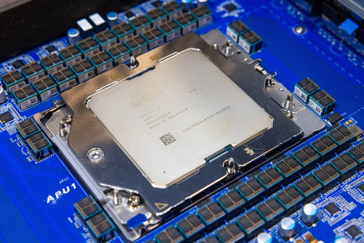
AMD Instinct MI300 (3.5D)
Compute chiplets stacked on I/O dies plus HBM on an interposer; MI300A joins CPU and GPU.
Image: ServeTheHome (Patrick Kennedy) · © ServeTheHome; no open licence · ServeTheHome (SC23, Nov 2023)


Contested: Multi-chip packaging predates 2011; Xilinx's 'first' claim comes from AMD's own slides, and AMD popularised 'chiplet' with Zen 2.