Photolithography (contact printing → DUV → EUV → High-NA EUV)
Printing circuit patterns onto wafers with light; the core manufacturing step whose resolution sets how small transistors can be.
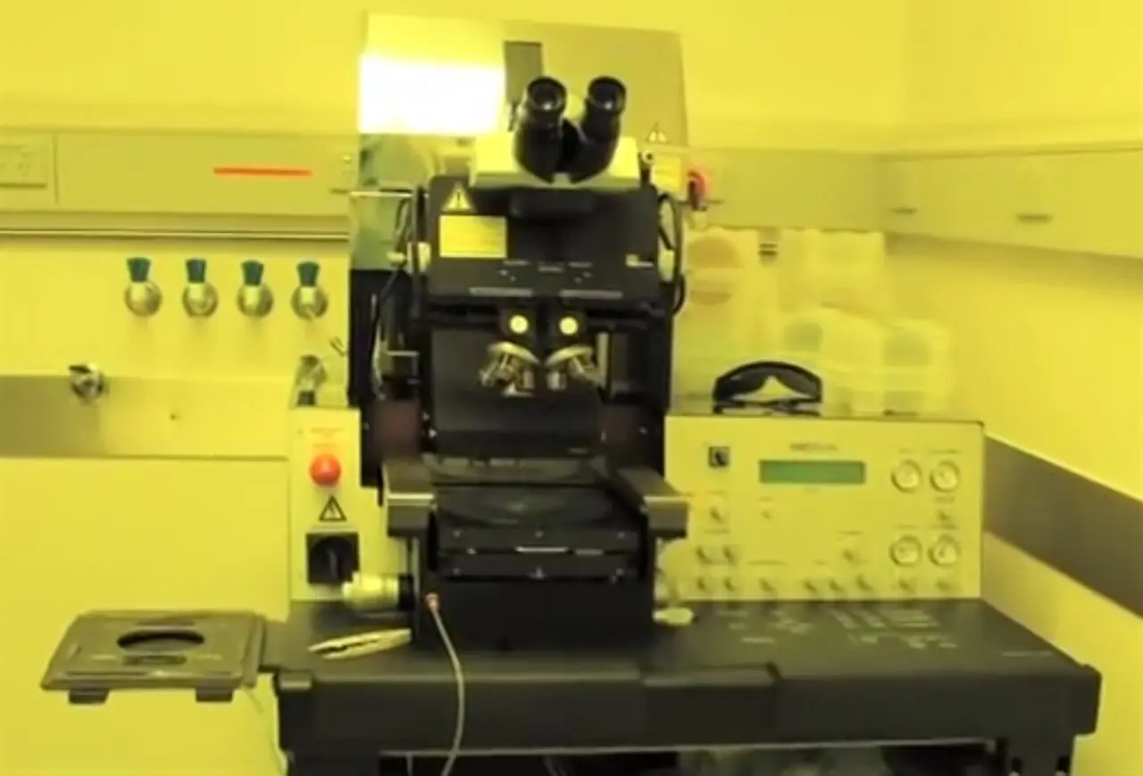
- 1955
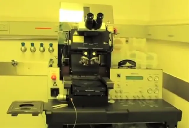
First version
Jules Andrus and Walter Bond (Bell Labs); Jay Lathrop and James Nall (US Army DOFL)
Image: James Friend · CC BY 3.0 · Later example (2012 contact mask aligner), not the 1955 apparatus · Wikimedia Commons - 1958

Step-and-repeat camera
Last and Noyce build a camera that prints many identical transistors per wafer.
Image: Fairchild Semiconductor Corporation (1958 advertisement) · Public domain (per Commons: US 1958 publication); trademark · Fairchild Semiconductor's first advertisement, Electronics (engineering edition), 15 August 1958, p. 26 (Commons scan, from americanradiohistory.com) - 1978
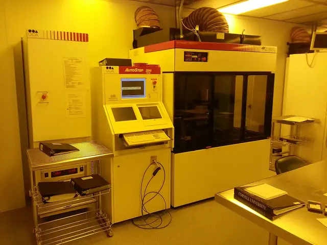
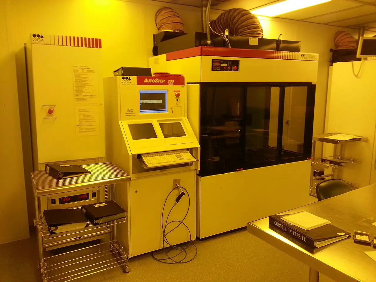
Wafer stepper (GCA DSW 4800)
Projects a reduced mask image onto one chip at a time, giving finer features than whole-wafer aligners.
Image: a13ean · CC BY-SA 3.0 · Wikimedia Commons - 1984
No available image 193nm projection lithography
MIT Lincoln Lab develops 193nm deep-UV projection (1984–96); dominant for decades.
- 2006
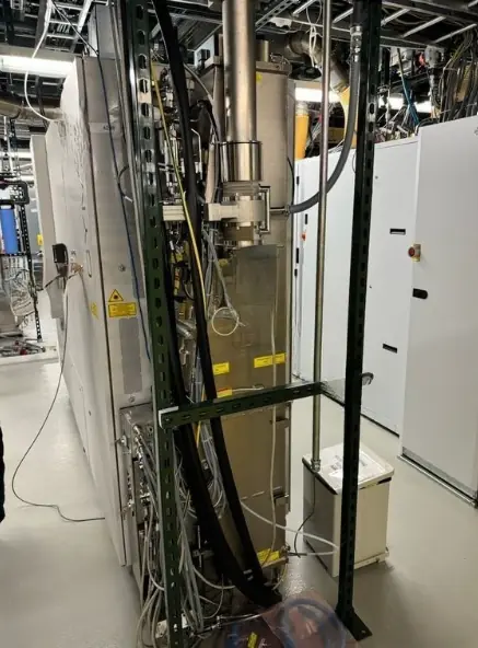
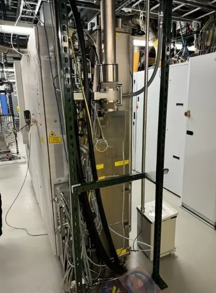
Immersion lithography
A layer of water between lens and wafer lifts numerical aperture above 1, so 193nm light prints features below 45nm; it carried chipmaking until EUV.
Image: Tara Semiconductor Technology · © Tara Semiconductor Technology; equipm… · Tara Semiconductor Technology equipment listing - 2019
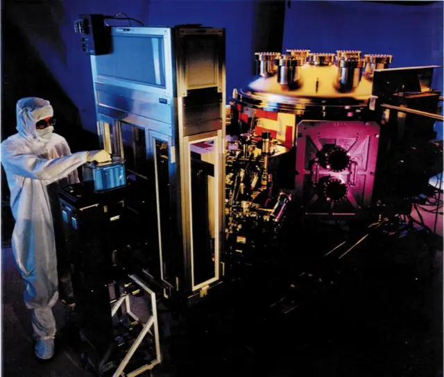
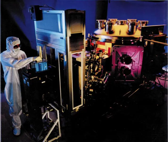
EUV in volume production
TSMC N7+ is the first EUV process delivering customer products in high volume.
Image: Lawrence Livermore National Laboratory · Public domain · Wikimedia Commons - 2026
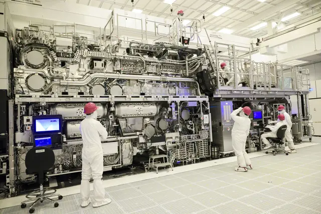
High-NA EUV in volume production
Larger 0.55-NA optics print finer lines; now used for select layers of some Intel Panther Lake chips in volume.
Image: Intel Corporation (press photo via Tom's Hardware) · © Intel; press image, no open licence · Tom's Hardware (Apr 2024)



Contested: Bell Labs (Andrus and Bond) adapted photoengraving to silicon in 1955; Lathrop and Nall patented photolithographic techniques at the Army's DOFL in 1957.