Planar process
Leaving protective oxide on the wafer keeps junctions sealed and flat, making reliable transistors and monolithic ICs mass-producible.
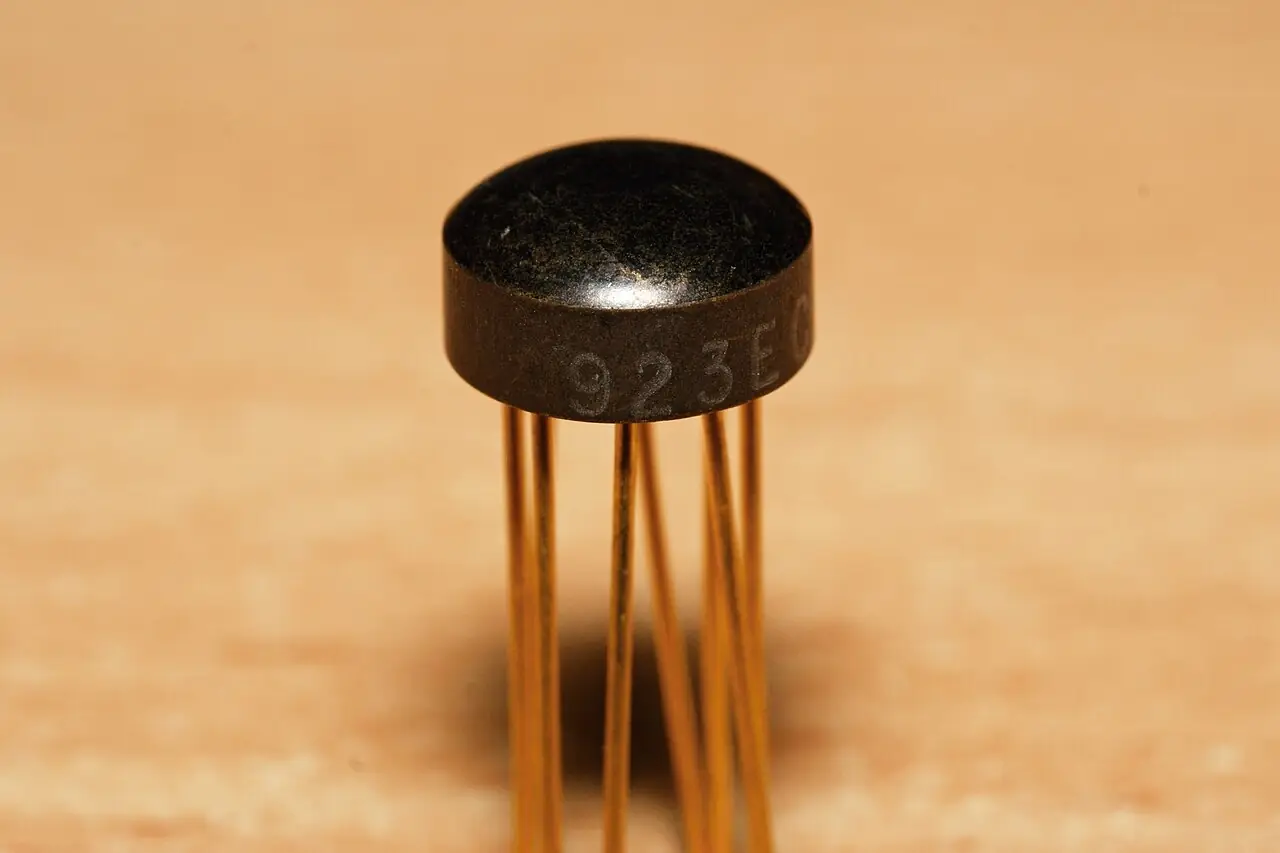
- 1959
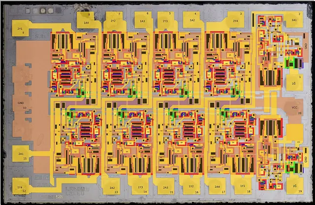
First version
Jean Hoerni (Fairchild Semiconductor)
Image: Robert.Baruch · CC BY-SA 4.0 · Wikimedia Commons - 1960
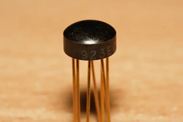
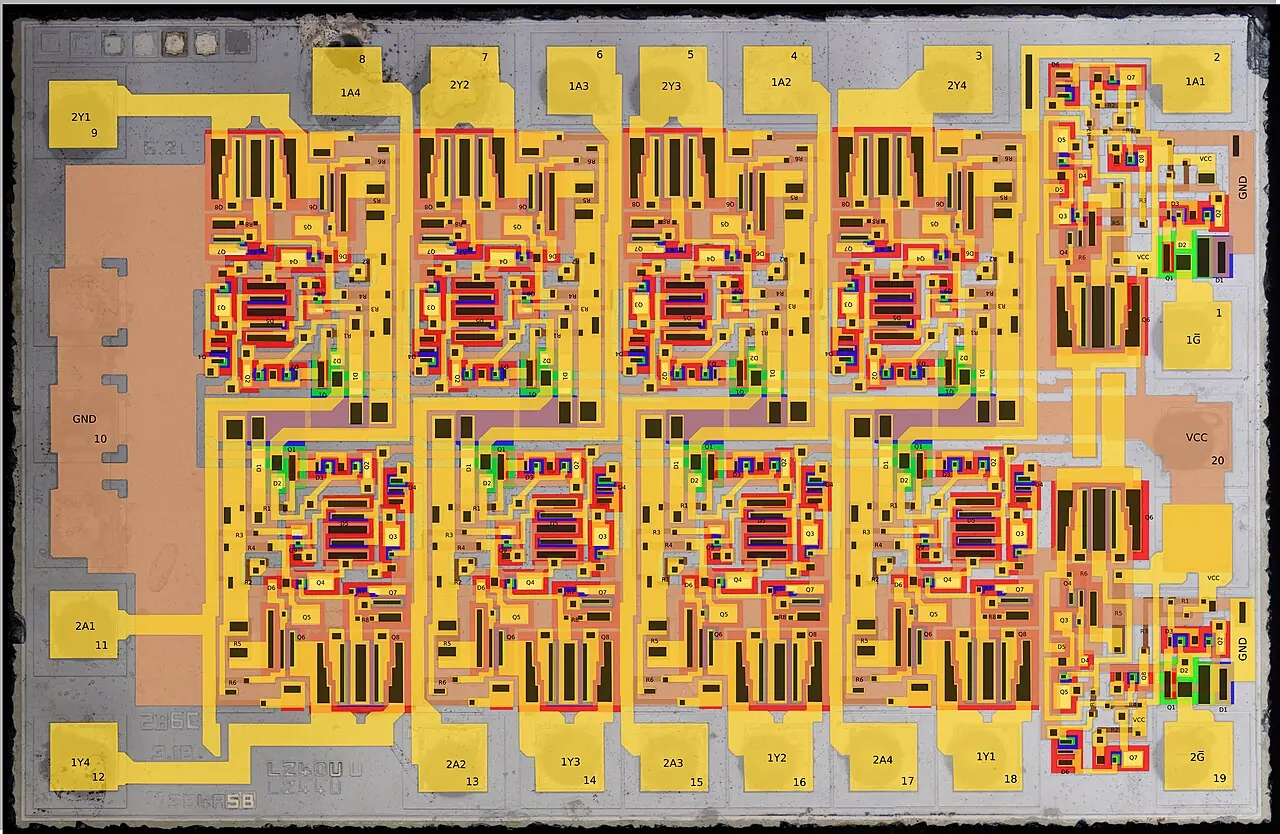
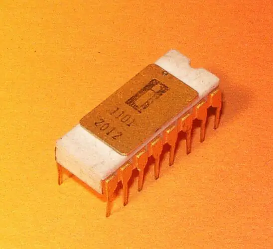
Planar integrated circuit
Noyce's monolithic IC built with aluminium interconnect laid over the protective oxide.
Image: 155LA3 · CC BY 4.0 · Wikimedia Commons - 1968
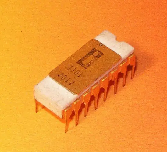
Self-aligned silicon gate
Polysilicon gate replaces aluminium, improving MOS density, speed and reliability.
Image: Christian Bassow · CC BY-SA 4.0 · Wikimedia Commons - 1997
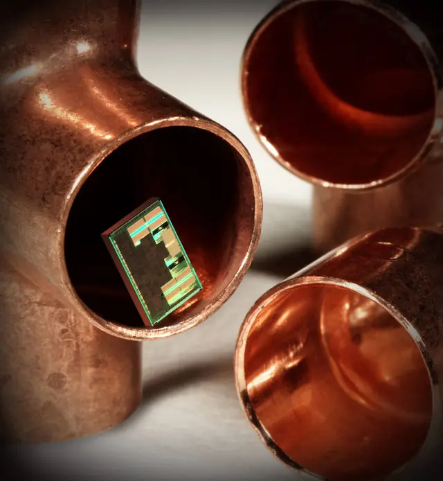
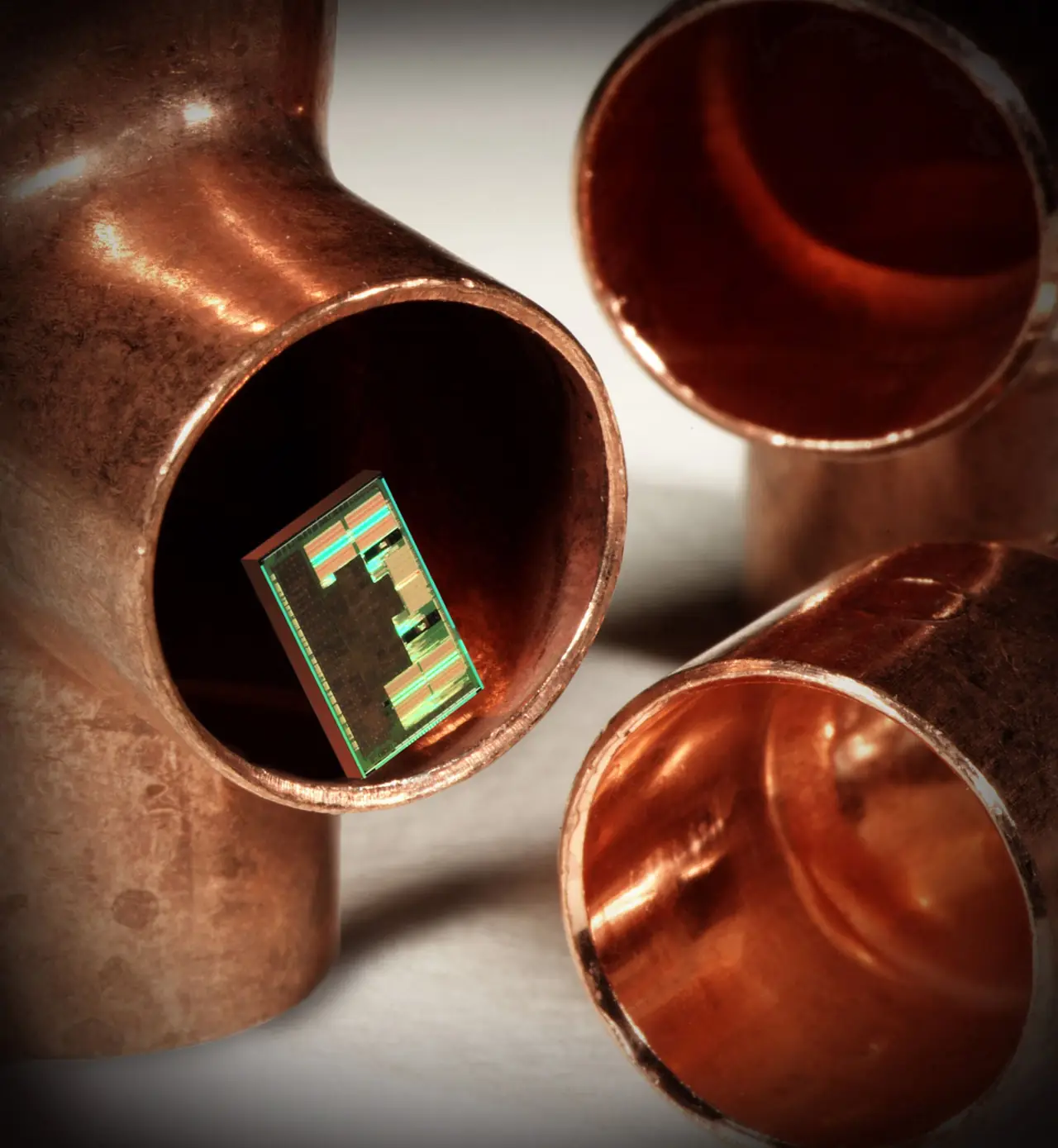
Copper interconnects
IBM replaces aluminium wiring with lower-resistance copper, speeding chips as wires shrink.
Image: IBM · © IBM; IBM Archives image, no open lice… · IBM History: Copper interconnects - 2007
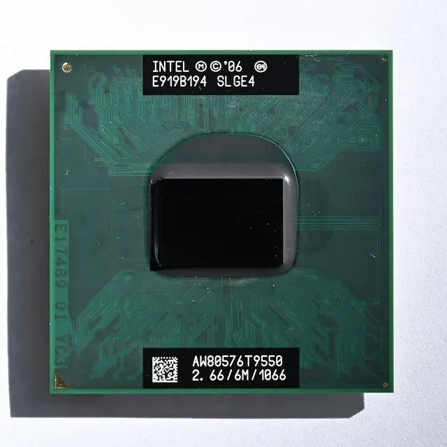
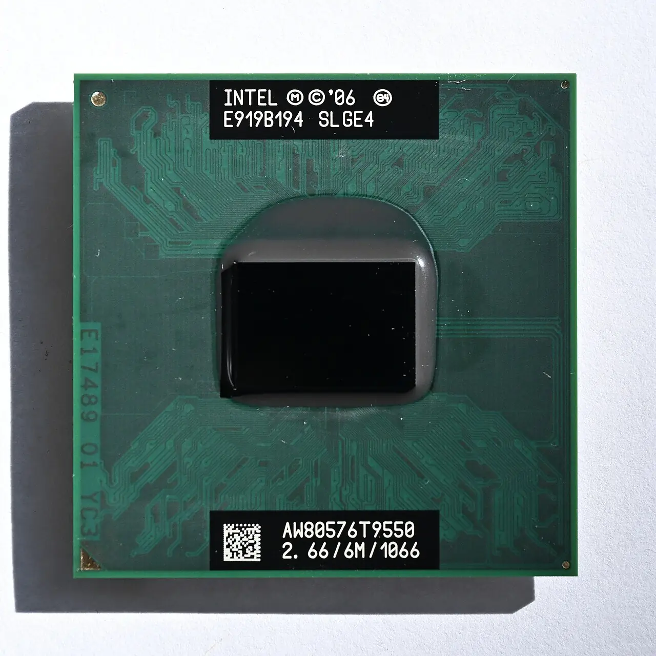
High-k metal gate
Intel's 45nm chips swap the silicon-dioxide gate insulator for hafnium-based high-k, cutting leakage.
Image: 4300streetcar · CC BY 4.0 · Wikimedia Commons - 2011
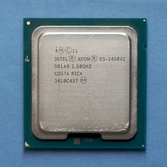
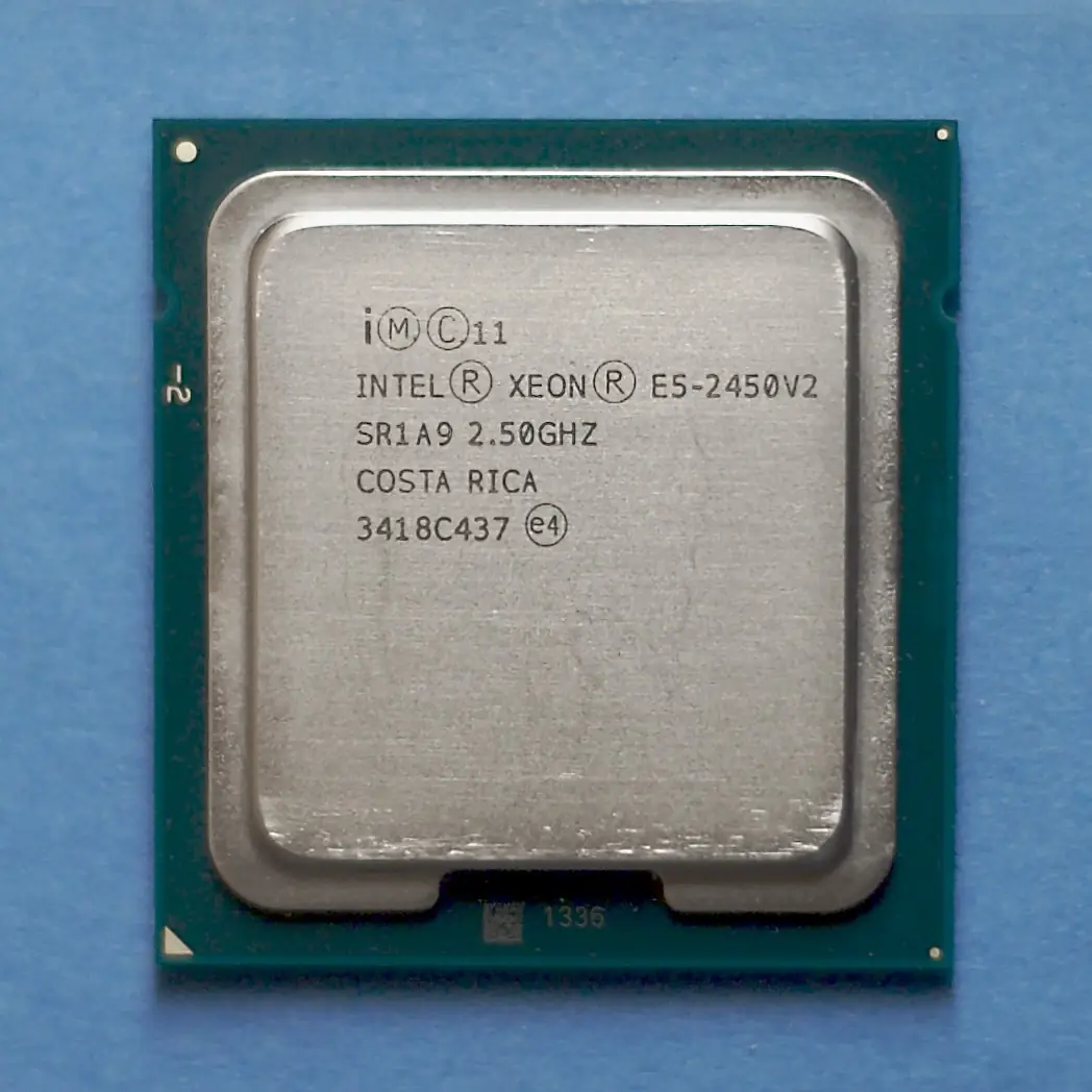
3D fin transistors (Tri-Gate)
Intel's 22nm channel rises from the flat surface as a fin, ending planar transistors at the leading edge.
Image: IrisChronomia · CC BY-SA 4.0 · Wikimedia Commons


Contested: Hoerni recorded the idea in December 1957 but developed it in 1959; Frosch and Derick's oxide masking at Bell Labs was a precursor.