High Bandwidth Memory (HBM)
Vertically stacked DRAM dies on a wide interface beside the processor; the memory bottleneck-breaker behind modern GPUs and AI accelerators.
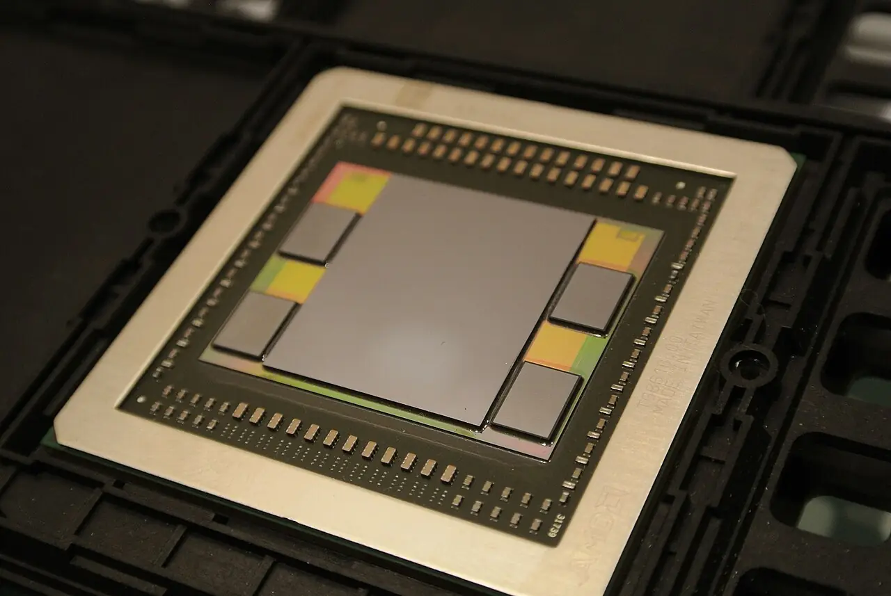
- 2013
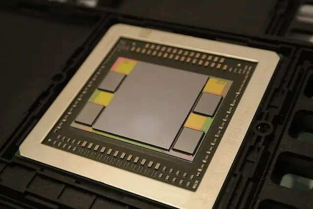
First version
SK hynix and AMD (JEDEC JESD235)
Image: C. Spille/pcgameshardware.de · CC BY-SA 4.0 · Wikimedia Commons - 2016
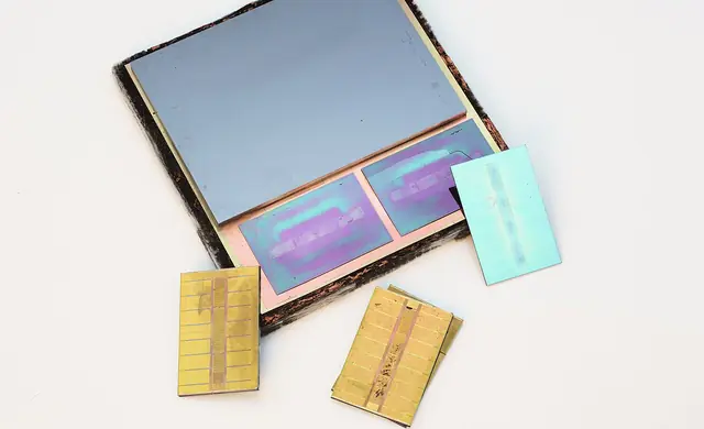
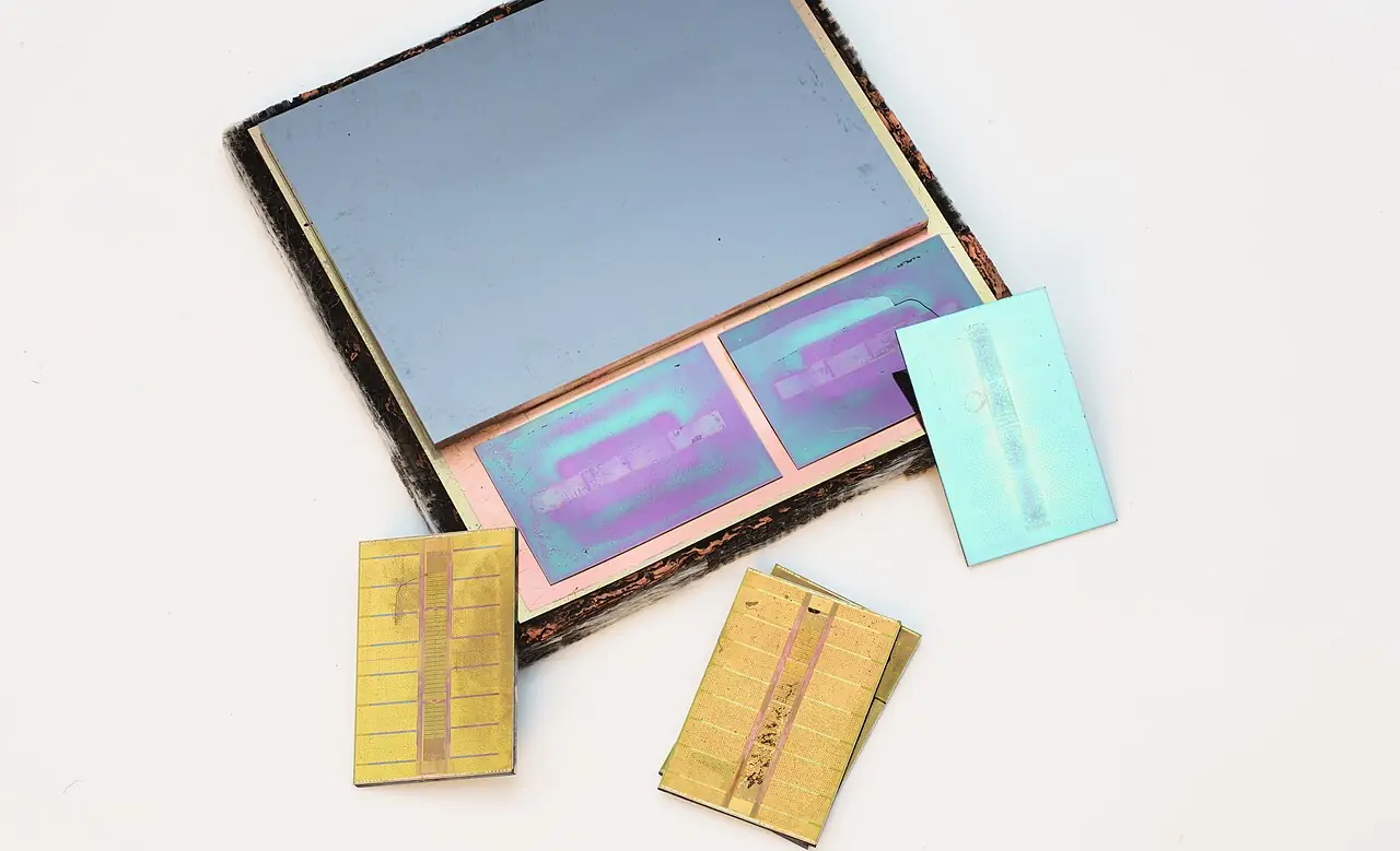
HBM2
Doubles per-pin speed and allows 8-high stacks; adopted in data-centre accelerators such as NVIDIA's Tesla P100.
Image: Fritzchens Fritz · CC0 · Wikimedia Commons - 2022
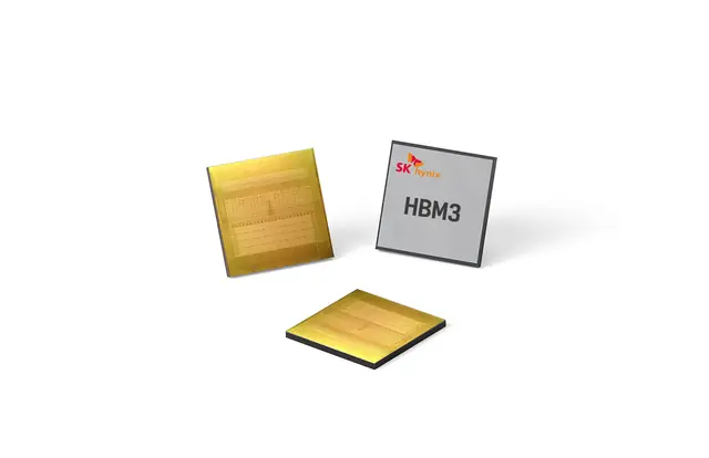
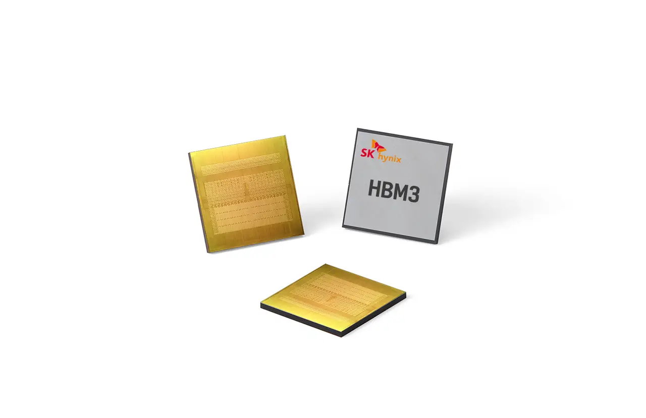
HBM3
Doubles independent channels to 16 and lifts pin speed to 6.4Gb/s, about 819GB/s per stack.
Image: SK hynix · © SK hynix; press image, no open licence · SK hynix Newsroom - 2025
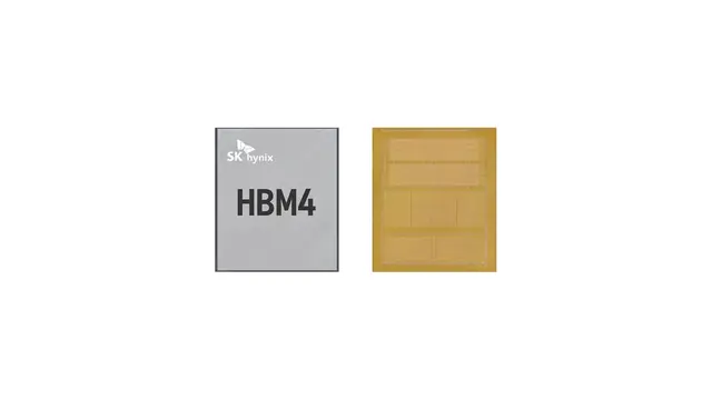
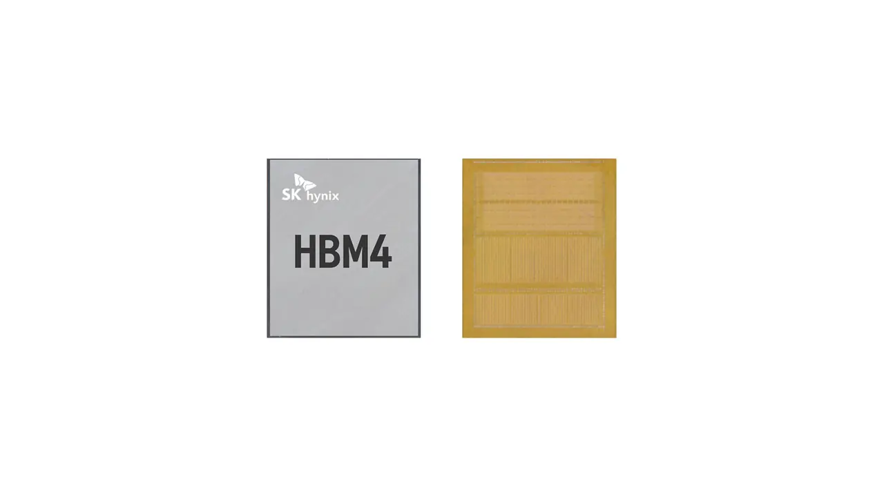
HBM4 standard
JEDEC JESD270-4 (April 2025) doubles interface to 2,048 bits.
Image: SK hynix · © SK hynix; press image, no open licence · SK hynix Newsroom (Mar 2025)


Contested: Firsts are disputed per generation: Samsung led HBM2 mass production; Samsung, Micron and SK hynix all claimed early HBM4 shipments in 2026.