Moore's law and process-node scaling
Prediction that components per chip double regularly as cost per function falls; it became the industry's roadmap for node shrinks.
- 1965

First version
Gordon Moore (Fairchild); scaling rules by Robert Dennard (IBM)
Image: Fairchild Camera and Instrument Corporation · Unclear; no licence stated (corporate wordmark, trademark; 1965 advertisement) · Electronics magazine, 19 April 1965 (vol. 38 no. 8), p. 14 Fairchild advertisement; worldradiohistory.com scan (PDF page index 15) - 1974
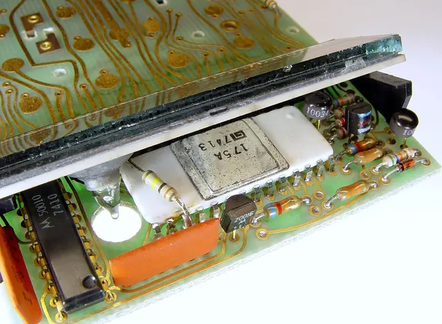
Dennard scaling
Rules for shrinking MOS dimensions make each node faster, cheaper and lower-power.
Image: Mister rf · CC BY-SA 4.0 · Wikimedia Commons - 1975

Revised pace
At IEDM Moore slows the projection to a doubling every two years.
Image: Pauli Rautakorpi · CC BY 3.0 · Wikimedia Commons - 2005

Multi-core era
Dennard scaling breaks down as clock speeds stall; extra transistors go into multiple cores per chip.
Image: Mckaysalisbury · CC BY-SA 3.0 · Wikimedia Commons - 2011
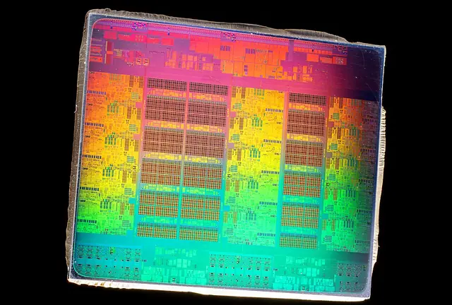
FinFET era
22nm Tri-Gate transistors keep scaling going as planar transistors run out.
Image: Fritzchens Fritz from Berlin · CC0 · Wikimedia Commons - 2019

EUV node
TSMC N7+ is the first EUV process in high-volume customer products.
Image: Bechology · CC BY-SA 4.0 · Wikimedia Commons - 2025

2nm class: nanosheets and backside power
Intel 18A pairs gate-all-around transistors with backside power wiring; TSMC N2 nanosheets also enter volume production.
Image: 极客湾Geekerwan · CC BY 3.0 · Wikimedia Commons





Contested: Moore's 1965 paper projected yearly doubling; in 1975 he slowed it to 'a doubling every two years'.