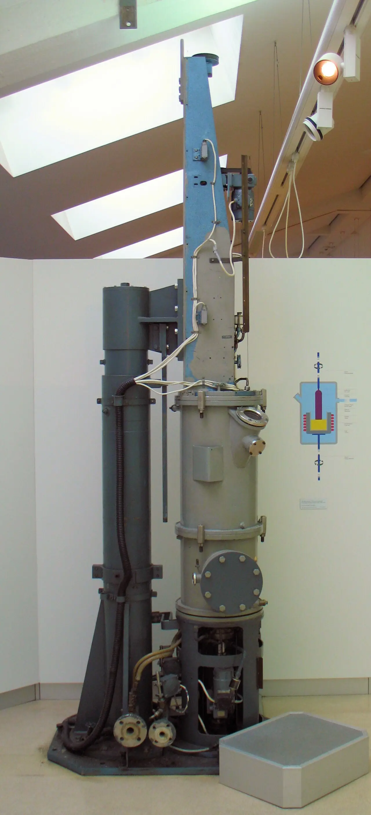
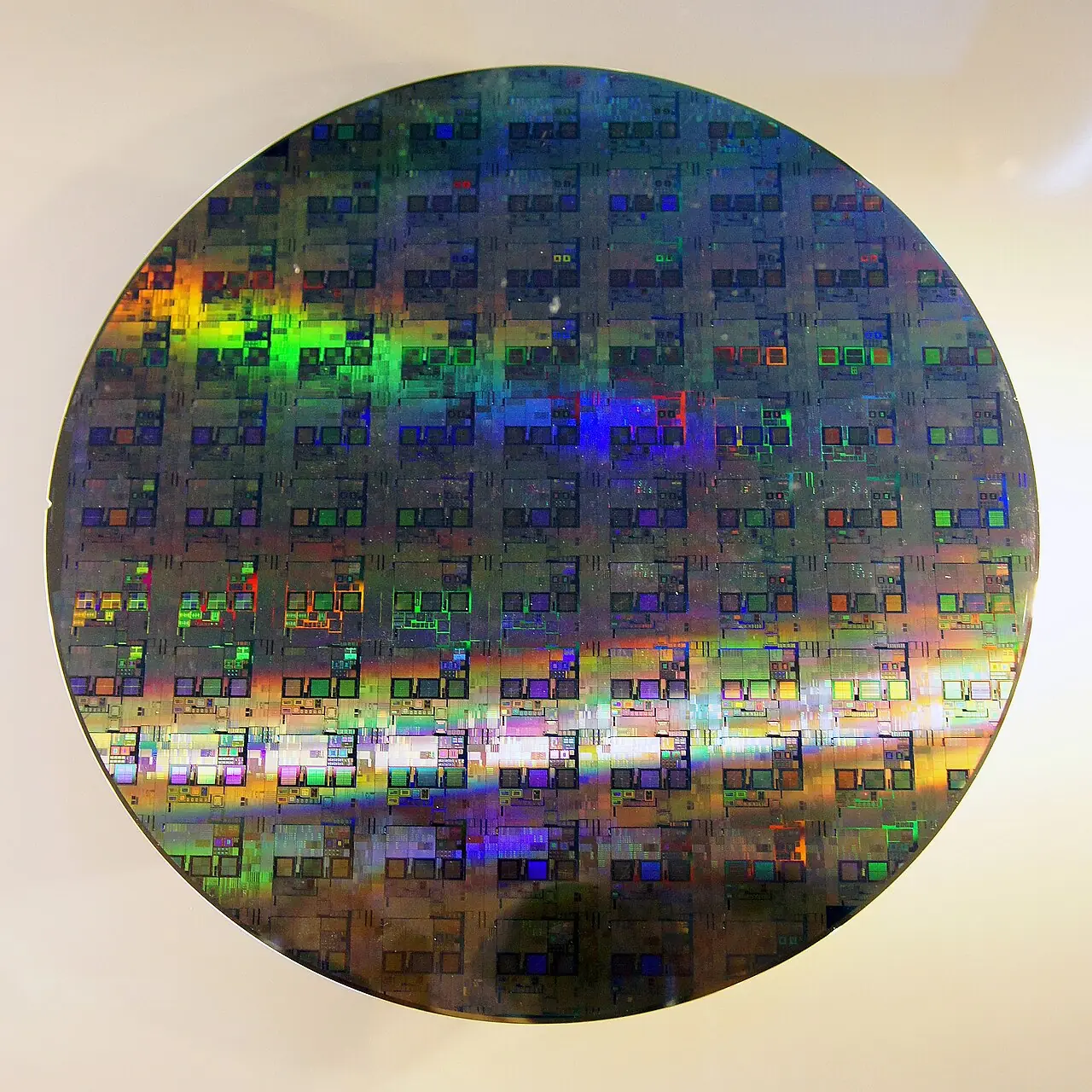
Single-crystal growth and ultra-pure silicon wafers (Czochralski method)
Pulling a flawless single crystal from molten material and refining it to parts-per-billion purity; about 90% of semiconductor devices start from crystals grown this way, sliced into wafers.
- 1916

First version
Jan Czochralski (AEG); Gordon Teal and John Little (Bell Labs); William Pfann and Henry Theuerer (Bell Labs)
Image: Peter Behrens · Public domain · Wikimedia Commons - 1950
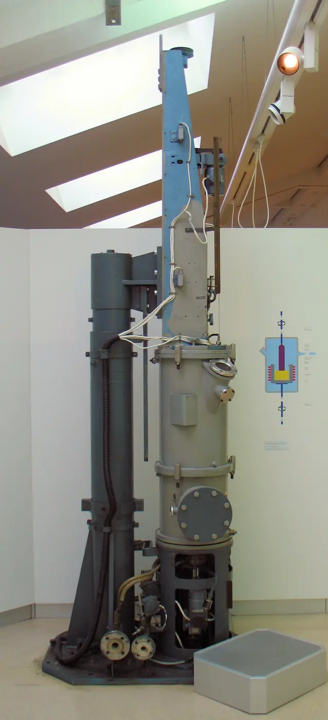
Single-crystal germanium for transistors
Teal and Little adapt crystal pulling to germanium, giving the uniform crystals that junction transistors need.
Image: Journey234 · Public domain · Wikimedia Commons - 1952
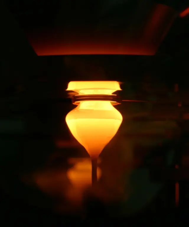
Zone refining and float-zone silicon
Pfann's zone refining and Theuerer's crucible-free float-zone method push silicon impurities below one part per billion by 1955.
Image: Matthias Renner · CC BY-SA 3.0 · Wikimedia Commons - 2001
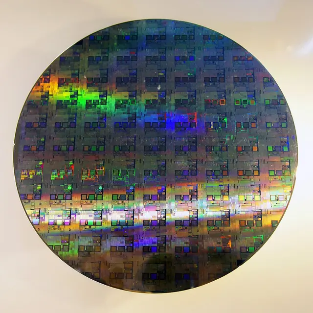
300 mm wafers in volume production
Infineon's Dresden fab, billed as the first to use 300 mm wafers, starts volume chipmaking on discs with 2.25 times the area of 200 mm wafers.
Image: Peellden · CC BY-SA 3.0 · Wikimedia Commons